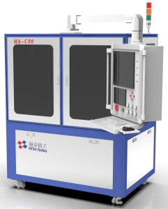
Equipment Introduction:
The Ceramic Substrate Defect Inspection Machine is mainly used for detecting appearance defects on ceramic substrates. This inspection machine employs a high-precision line scan camera; for ultra-high-precision inspection, it utilizes a high-precision line scan laser profiler to perform 3D scans of the substrate surface. It is paired with HiTel’s vision algorithm specifically developed for ceramic substrate materials to conduct in-depth analysis of 2D imaging, 3D point clouds, and depth maps. This enables efficient and accurate detection of defects such as concavity, convexity, scratches, breakage, and spots on the substrate surface, achieving industry-leading levels in both detection rate and detection accuracy.
Core Parameters :
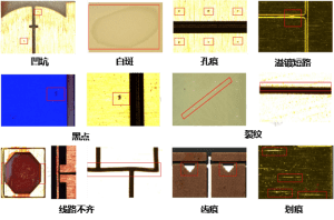
• Appearance: It can detect defects such as pits, bumps, ceramic marks, defects, spots, pores, and cracking on the substrate;
• Ceramic Marks: It can detect ceramic substrates with ceramic mark heights of 0.01mm-0.03mm, with a quantity requirement of 1/5cm²;
• Wrinkles: It can detect substrates with wrinkle heights of 0.025mm-0.03mm, with a quantity requirement of 1/5cm²;
• Burrs: It can detect ceramic substrates with burr heights of 0.01mm-0.025mm, with a quantity requirement of 1/5cm²;
• Marks: It can detect ceramic substrates with mark edge lengths of 10mm and depths of 0.02mm, with a quantity requirement of 1/5cm²;
• Pores (Pinholes, Pockmarks): It can detect ceramic substrates with pore diameters of 0.04mm-0.15mm, with a quantity requirement of 1/5cm²;
• Spots: It can detect ceramic substrates with spot diameters of 0.12mm, with a quantity requirement of 1/cm²;
• Defects: It can detect ceramic substrates with defect widths of 0.7mm and depths of half the thickness, with a quantity requirement of 1/cm².
Application Expansion :
Copper-Clad Ceramic Substrate Inspection (referring to special process boards where copper foil is directly bonded to the surface of ceramic substrates under high temperature), IGBT Front-End Production Inspection, SiC Substrate Inspection.